





CTK CTKG100N10DF5 100V/100A N-Channel Power MOSFET | Official Release

CTKG100N10DF5 100V/100A
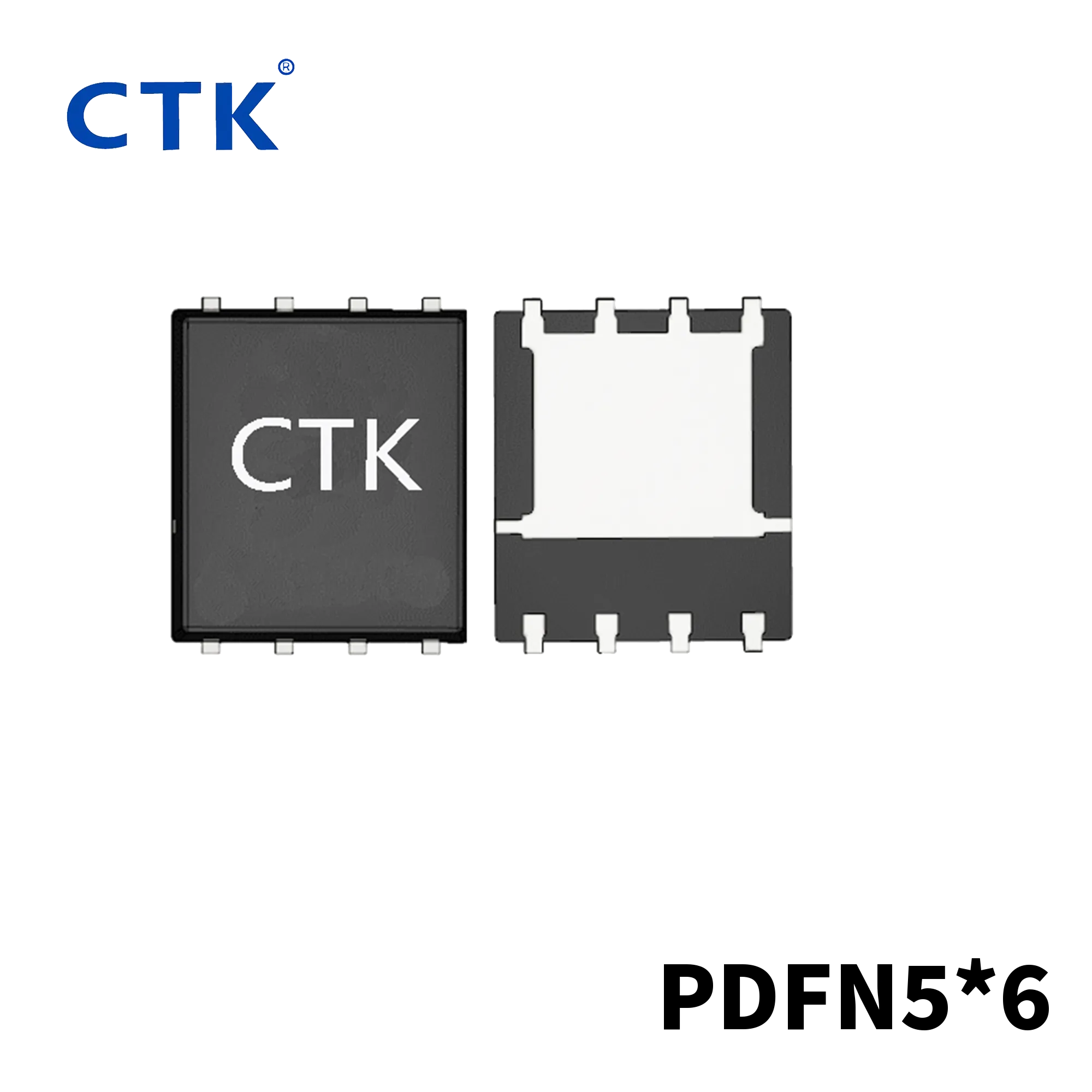
N-Channel Power MOSFET · Advanced Split-Gate Trench · PDFN5×6-8L SMD
| Brand | CTK (Dongguan Tongke) |
| Model | CTKG100N10DF5 |
| Type | N-Channel · Split-Gate Trench |
| VDS | 100V |
| ID | 100A |
| RDS(on) | 6.5mΩ (typ.) @ VGS=10V |
| Package | PDFN5×6-8L |
The CTKG100N10DF5 is an N-channel power MOSFET designed for high-current, high-efficiency, and high-reliability power applications. Built on advanced split-gate trench technology, it delivers low conduction loss, robust switching performance, and excellent thermal behavior in a compact surface-mount package. Ideal for power conversion, load switching, motor drives, battery management, and industrial systems.
Core Electrical & Design Advantages
Ultra-Low On-Resistance
Typical 6.5mΩ @ VGS=10V. Minimizes conduction losses at 100A, reduces temperature rise and simplifies thermal design.
Split-Gate Trench Process
Balances RDS(on) and gate charge Qg for high-frequency PWM operation with low switching loss and improved EMI.
100% Dual Reliability Screening
100% UIS avalanche test + 100% ΔVds dynamic voltage stress.Withstands spikes,back-AEMF,and transients.
Integrated Body Diode
Built-in fast-recovery diode supports freewheeling in bridge and buck/boost circuits, reducing external components and BOM cost.
PDFN5×6-8L Compact Size
Only 5×6mm, over 60% smaller footprint than TO-252/TO-220, ideal for slim and space-constrained designs.
Exposed Thermal Pad
Large bottom pad transfers heat directly to PCB copper. Maintains controlled temperature rise even at 100A continuous current.
8-Pin Multi-Path Current Distribution
Parallel drain/source pins improve current capability and reduce parasitic inductance for high-frequency stability.
Standard Pin-to-Pin Footprint
Industry-standard pad layout enables direct replacement of similar MOSFETs without PCB redesign, speeding up iteration.
Key Application Areas
Load Switch
Power stations, PD chargers, BMS, hot-swap
PWM Power
Buck/Boost, inverters, BLDC drives
Industrial & Automotive
AC-DC, auxiliary power, UPS, servo
Outdoor power stations / lithium battery charge/discharge main switches
High-power synchronous Buck and Boost DC-DC converters
Industrial AC-DC power supplies and communication power module
High-power PD chargers and multi-port adapter power path control
Micro photovoltaic inverters and small DC inverter systems
Automotive auxiliary power and high-current distribution circuits
BMS overcurrent / overvoltage / short-circuit protection switches
BLDC motor controllers for power tools and home appliances
UPS backup power and servo driver output stages
Hot-swap and power distribution in industrial control & robotics
Speed controllers for electric vehicles and light EVs
High-power LED drivers and industrial power modules
Package & Production Advantages (PDFN5×6-8L)
Small footprint, high density
5×6mm standard DFN, suitable for slim industrial and e-mobility controllers.
Bottom thermal pad
Direct heat transfer to PCB copper via exposed pad, supports 100A continuous operation.
8-pin multi-path current
Parallel D/S pins reduce parasitic inductance and enhance high-frequency stability.
PIN1 marking + standard pad
Prevents reverse placement; compatible with similar MOSFETs for drop-in replacement.
Mature SMT process
Fully automated pick-and-place, high reflow yield, stable mass production.
Clear marking
"CTKG100N10DF5" for easy IQC incoming inspection and traceability.
Packing & Supply Information
13-inch standard tape & reel
5,000 pcs / reel
50,000 pcs / carton
Standard taping, compatible with automatic placement
Supply chain advantage: stable factory delivery, direct replacement for imported brands, optimized BOM cost.
Selection Summary
The CTKG100N10DF5 combines a 100V/100A rating, 6.5mΩ ultra-low on-resistance, split-gate trench technology, and 100% dual avalanche screening. Housed in the compact PDFN5×6-8L package, it addresses thermal design, surge immunity, and board-space challenges while offering pin-to-pin compatibility, stable production, and reliable supply. It is an excellent cost-performance N-channel MOSFET for consumer fast charging, portable energy storage, industrial control, automotive power, and power tools.